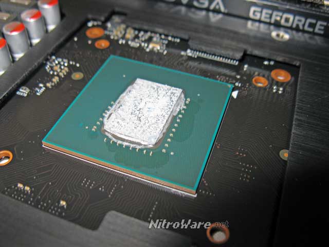
Maxwell GM206 GPU - a smaller chip for cost and efficiency.
Like their card/board models, NVIDIA also assigns a numerical model number to their GPUs. A 6 is usually the companies 2nd or 3rd best chip in the product stack. GM206 carries over all the goodness from GM204 (GTX980/970) such as Colour and Memory compression, DirectX 12, Multi-Frame Sampled Anti-Aliasing(MFAA), Voxel Global Illumination (VXGI), HDMI 2.0, H265 hardware support, lower temps/power consumption and a improved video engine. G-Sync, DSR and GPU Boost are there as standard.
Apart from being half of a GM204, comprising half the compute units and memory controllers the only change is with NVIDIA's NVENC video engine, comprised of proprietary silicon that's not part of the 3D pipeline. For GTX 980, hardware h265 aka HEVC CODEC support was promised and enabled in the video drivers however the software to support it was not available and NVIDIA did not say much about the subject at launch. We were not able to test this functionality during out time testing the GTX 980 at launch.
NVIDIA have now stated GM206 has full h264 encode/decode support while GM204 will have h264 encode only. This is disappointing for those already with a 980/970 but good news for potential 960 owners as the functionality is confirmed. However again supporting software is required. The launch GPU having a bug or regression with the video hardware is not without precedent. The 8400/8600 follow-up to the 8800 included a significantly upgraded video engine and deleted the need for a separate 'i/o' chip that was necessary for the higher end parts, the 6600 also had upgraded video support compared to the original 6800 launch model.
Unlike GTX 970, the design for GM206 and GTX 960 is straight foward and does not utilise any workarounds for memory access as all hardware units in the chip(exactly half the full GM204/GTX 980) design are available for use. We measured slightly above 2GB usage in our testing, being able to fully utilise the 2GB frame buffer on the card.
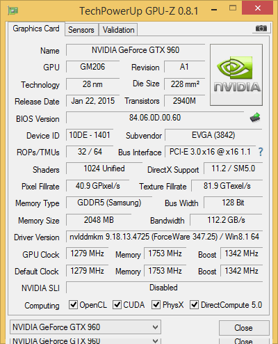
Being the half-design it is, GM206 is actually physically small being only 227mm2, rather than being the larger chip with half the cores disabled. This is done to ensure the optimum yields of chips. If GM204 had been used for the GTX 960, many otherwise more expensive working chips which could have been used in GTX 970 or GTX 980 cards would have been wasted, driving costs up and production down.Thermals would not be optimum either due to the variance of disabled and enabled cores. A further side effect of selectively enabling cores on the bigger GPU chip to meet a market segment also runs the risk of segmented/asymmetrical memory access, which is currently extremely controversial for the GTX970.
GM206 will be able to support larger memory capacities due to unused solder pads on some of the GTX 960 samples we have seen. For GTX 960 specifically, it does not have the horsepower to run games at 4K with high to ultra details so the extra memory may be debatable.
By making a dedicated smaller chip, although with a large upfront cost to design allows NVIDIA to optimise production costs and yields, therefore maximising availability of all three 2nd gen maxwell Desktop GPUs to market. GM206 is smaller and therefore more dense than GM204 packing in , which means higher temperatures when the chip is working hard, although smaller than GTX980 the EVGA over clocked sample we tested did reach to the high 70s in load testing, and 80s when over clocked.
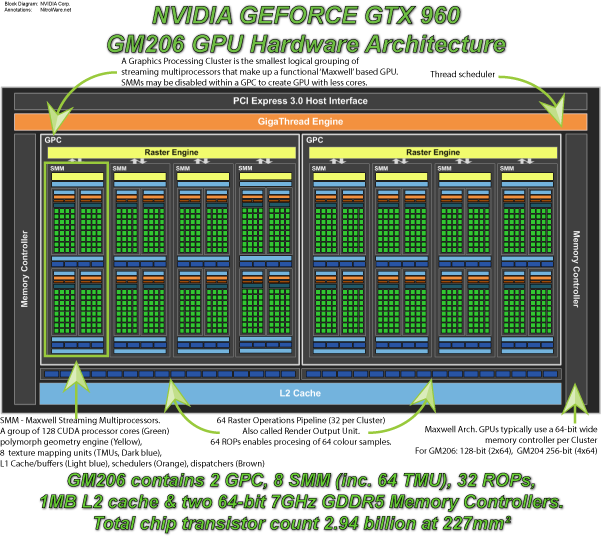
Explaining and Understanding the actual CUDA/shader cores and the low level functionality of a graphics pipeline is beyond the scope of this review but we can still discuss the logical blocks and modules that make up a modern programmable GPU. You may hear talks of 'cores,clusters, TMUs and ROPs' and while finite understanding is not necessary, understanding their place in a GPU logically can visualise the differences between smaller and larger GPUs. We have annotated NVIDIA's standard GPU block diagram of maxwell to highlight each module.
Although we talked about the fundamentals of the Maxwell architecture, the block diagram only represents the 'compute core' of the GPU, there is other logic that is not illustrated such as the NVENC video engine, display controllers, power management, crossbar interface between the different functional nits and telemetry all of which combine to make a GPU. These need to be taken into account when considering the transistor count for the chip. The transistor count for this logic is constant between different GPU designs of the same family.
At launch time, the following NVIDIA partners have boards ready
- ASUS - STRIX
- EVGA - ACX 2.0 cooler line Reference Single fan, Superclocked single fan, Reference dual fan, Superclocked dual fan, Super Superclocked dual fan, For the Win dual Fan (single fan models are short PCB for compact systems)
- Gainward - Overclocked Reference, Phantom dual fan, Phantom dual fan golden sample
- GALAX - Reference, Dual Fan OC, Dual Fan EXOC
- Gigabyte - Triple fan G1 Gaming
- Inno3D - Dual Fan HerculeZ X2, Triple fan iChill
- MSI - Reference, Dual Fan Armor, Dual Fan Gaming, Dual Fan 100 Mil Edition.
- Palit - Reference, Dual fan Jetstream, Dual fan Super Jetstream
- PNY - Reference (XLR8)
- POV - Reference (Trooper), Reference OC(Trooper Ammo)
- Zotac - Dual Fan, Dual Fan AMP! (OC)
Overall NVIDIA claims GTX 960 is 50% faster than GTX 660 and 2x as power efficient, deep down, each GM206 Maxwell CUDA core is claimed to be 1.4x faster than a GK106 Kepler CUDA core and 2x performance per watt.
Multi-Frame Sampled Anti-Aliasing performance
One of the crown jewels of the 2nd Gen maxwell GPU family is MFAA, being a feature implemented on the GPU allowing anti aliasing patterns to be changed, promising a algorithm to deliver MSAA like quality at higher performance
We could not test this with GTX 980 as it took many weeks for the driver to be released and our card was returned before driver availability. When a driver was made available, the 'whitelist' of MFAA supported games was minimal and while the tech on paper was promising, the implementation led some to see the feature as a gimic.
With the launch of GTX 960,NVIDIA has changed this. The white list is gone, all DirectX10/11 games that support MSAA will work with MFAA with the exception of Dead Rising 3, Dragon Age 2 and Max Payne 3 as of Jan-2015. This is great news and opens the door for added performance for thousands of titles.
NVIDIA promotes enabling MFAA with ease of one click using GeForce Experience however we do not see MFAA listed for all detected games. It is listed for Dirt3, Hitman Absolution, War Thunder, PlanetSide2, Crysis3, Battlefield but not Bioshock,Metro or either Batman.
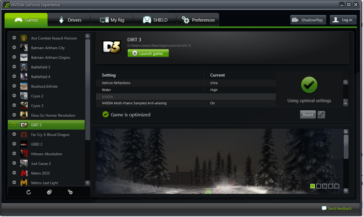
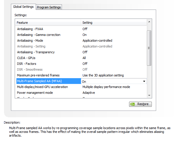
An additional override is provided in the NVIDIA control panel, forcing MFAA on for all MSAA software.
In Dirt 3 at 1200p Ultra 4X, Enabling MFAA on top of the in-game MSAA setting results using GFE in 108.83 FPS Minimum versus 102.8 for standard MSAA
In Hitman Absolution at 1200p Ultra 4X, Enabling MFAA using the driver override switch gave us Min 29.126/AVG 35.433/Max 46 versus min 29.126 avg 36.66 max 44.66 for the standard setting.
To be fair, NVIDIA promote MFAA has giving the most benefit the higher the resolution, especially at 4K. This is just a highlight here and further report will dive into more details with MFAA.
